


Dunlee is a brand of the Philips Company Group and distributes all products, solutions and services for the third-party imaging business. The product portfolio includes CT, MR and X-ray solutions for OEMs and 3D printed tungsten products.
© 2017 - 2025 Koninklijke Philips N.V. All rights reserved.
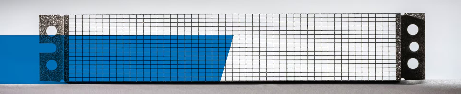
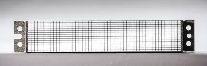
Tungsten, prized for its density and durability, is of increasing interest to manufacturers in a variety of markets, particularly because additive manufacturing is expanding its potential applications. As owner of the world's largest printer park dedicated to tungsten, Dunlee is at the forefront of developing products and components with this useful material.
Determining the right material for your product or component begins by assessing a material’s property specifications and comparing those to the needs of your product. If you need a material that offers any of these characteristics, then tungsten is worthy of your consideration.
Contact a Dunlee consultant to discuss if tungsten is right for your application.
| Radiation absorption | Density of 19.3 g/cm³ (1.7 times higher than lead) |
|---|---|
| Heat resistance | Extreme heat resistance and a melting temperature of 3422° C |
| Tensile strength | Above 1650° C |
| Long life | High resistance to wear |
| Sustainable | 100% recyclable |
| Magnetism | None |
One of tungsten’s advantages is its ability to be used in products of diverse sizes and tolerances. The tolerances listed are guidelines only; they vary based on design and application. Please contact Dunlee at [email protected] to discuss your needs.
| Maximum size | 230 x 230 x 200 mm (larger possible through innovative solutions) |
|---|---|
| Feature positions | 25 µm within an area of 50 x 50 mm2 30 µm within an area of 100 x 100mm2 50 µm within an area of 150 x 150 mm2 (maximum build area; dependent on design and tolerances) |
| Wall thickness | Minimum of 80 µm walls with 25 µm tolerance |
| Surface roughness | Assume an Ra of 6.3 after post-processing |
| Parallelism | 50 µm for wire EDM defined surfaces* |
| Flatness | 50 µm for wire EDM defined surfaces* |
*Impacted by overall outside dimensions
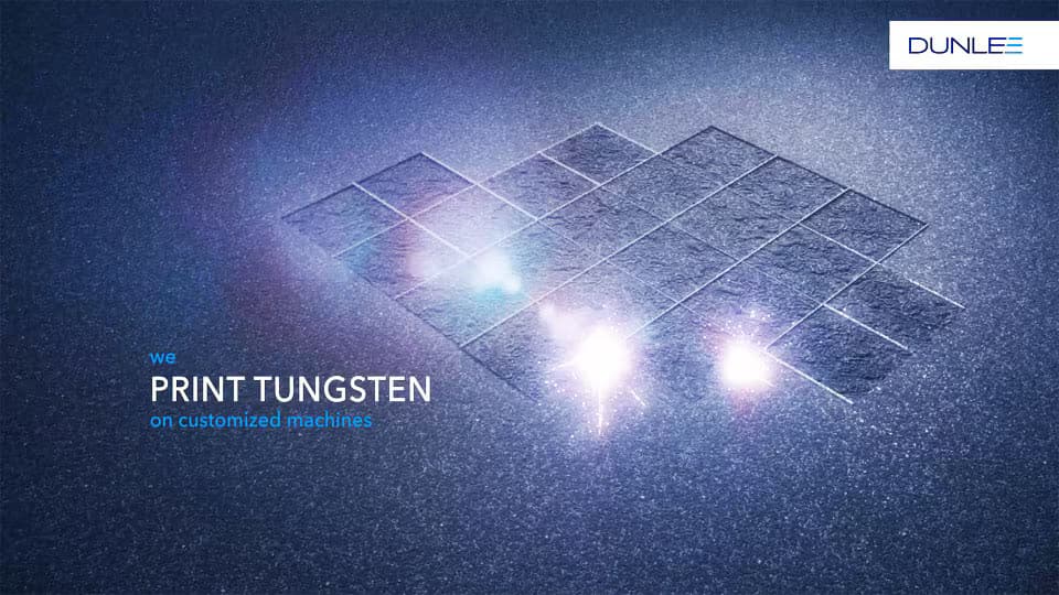
If you’d like to discuss a potential application for additive manufacturing with tungsten or if you’d just like to learn more about its properties, just send us an email at [email protected] and a member of our business development team will contact you.
